The a little history on band-gap voltage sources
and how they brought a kind of "Relativity" to analog
IC design is needed here. A very good article on band-gaps
by Bob Pease can be found at the following site.
http://www.national.com/rap/Application/0,1570,24,00.html
The term "Relativity" refers to band-gaps providing a
new way
of designing analog circuits around
ratios, ratios in terms of
transistor currents, or areas, or both, or voltages, or even
including resistors.
^ VCC VCC ^
/_\ /_\
_|_ _|_
/ _ \ / _ \
I1 \/ \/ \/ \/ I2
/\_/\ /\_/\ Vbe1 = (KT/q)ln(I1/Isat)
\___/ \___/
| |
____| <--------> |____
+ | _| Delta_Vbe |_ | +
Vbe1 |_|'A1 A2 `|_| Vbe2 = (KT/q)ln(I2/Isat)
|`-> <-'|
- |____________| -
_|_
///
What defines the emitter base voltage on an NPN
transistor is not easily controlled. The doping levels,
profiles, etc, determines this. It is modeled as a saturation
current used to define the emitter base voltage. This value
will vary from wafer to wafer and even across the wafer.
Vbe = (KT/q)ln(I_emitter/Isat)
When two NPNs are on the same chip, the relative difference
between two emitter base voltages is much better
controlled. In fact relative voltage differences
can be modeled just as being a ratio of two emitter areas.
Delta_Vbe = (KT/q)ln(A1/A2)
With enough cross coupling, transistor pairs like
the LM394 have been able to control the area ratio
match to be under 0.2%.
Delta_Vbe = (KT/q)ln(I1/I2) = (KT/q)ln(A1/A2)
But the ratio is actually a ratio of two
emitter current densities. So ratio in areas is the
equivalent of ratio in currents. So when bipolar
transistors can be layout out very well, a
dimension less number of ratio either in terms of
area, or current, or both can be counted on to produce
a voltage with is insensitive to IC processing and
will accurately track absolute temperature.
Bob Widlar was first to exploit this opportunity.
For the LM113 circuit above, he had made transistors
Q1 and Q2 two different sizes, and is counting on the
the voltage across R5 to be about following.
Delta_Vbe = (KT/q)ln(I_q1*A_q2/(I_q2*A_q1)
But a much easier way to see what he was doing is
to look at a Brokaw cell.
^ Brokaw, P., "A simple three-terminal IC bandgap reference",
IEEE Journal of Solid-State Circuits, vol. 9, pp. 388–393, December 1974.
Assuming the Op Amp is forcing both NPN's to draw
the same current, then the voltage across R1 should
be set by the 10E to the 1E emitter ratio.
Delta_Vbe_@R1 = (KT/q)ln(A1/A2) = (KT/q)ln(10) = 60mV
If R2 is five times larger than R1, then about 1.2V
should appear across R4. Room temperature is often
defined as 300K (27C). So the voltage across R2 is
effectively twice absolute temperature in terms of
millivolts. (600mV)
^
/_\ VCC
|
_|_
/ _ \
\/ \/
/\_/\
\___/ ___
|_____|VBG| 1.2V
_|_ |___|
\ /
_V_
|
_|_ +
/KTq\
\___/ 600mV
_|_
/// -
What Widlar discovered, was that when you add a diode
voltage in series with a voltage source which is twice
absolute temperature in terms of millivolts, the result
is a 1.2 voltage source which is almost independent of
temperature. And the voltage level comes close to the
band-gap voltage for silicon.
^ VCC
/_\ R1 7V +3.5mV/C_deg
|__/\ /\ /\___ ___
\/ \/ | |REF|
_____ | |___|
| _| | _|
|__|'QN1 |___|'QN2
_|_ |`-> | |`-> -2.2mV/C_deg
/// |__| |
|
_/\ /\ /\_| +20%/100C_deg
_|_ \/ \/ R2
///
It may not be appreciated what kind of impact this
band-gap had on how analog integrated circuits are now
biased. Before the band-gap, NPN transistors were reverse
biased to generate a zener voltage reference. Zeners
required at least a 7 volt supply. They were noisy.
Their TC was +3.5mV per degree C. The TCs of the diodes
also needed to be taken into account to generate a
reference current source to bias up everything.
^
/_\ VCC < 1V
______|_______
| |
-> PNP <-
QP2 `|______|' QP1
_ '| | |`_
| |_____|
|____ | Delta_Vbe_@R1 = (KT/q)ln(10) = 60mV
|_ | NPN _|
QN1`|_|_____|' QN2
<-'| |`->
| 10X |
_|_ |
/// <--1uA |
__/\ /\ /\_|
| \/ \/
_|_ R1 60K 60mV
///
Gnd Iref = Delta_VBE/R1
Now analog circuits can be biased up below 7 volts.
The circuit above is effectively a current limiting
SCR. This circuit will regenerate until the gain from
QN1 to QN2 is exactly one. Notice that it requires little
more than a diode voltage of supply. The bias current
can be derived from the 60mV being expressed across
R1.
But things don't stop here. Widlar discovered that
band-gap reference currents can be used to area scale
transistors using resistors.
Delta_Vbe_@R1 = (KT/q)ln(1000,000) = 360mV
^
/_\ Delta_VBE/Rbias
_|_ 2uA
/ _ \
\/ \/ | 1pA ___
/\_/\ v | |OUT|
\___/ 1uA -> v |___|
|____ |
|_ | R1 360K _|
QN1 `|_|__/\ /\ /\___|'QN3
<-'| | \/ \/ | |`-> 1X
1X | | ______| _|_
_|_ | _| ///
/// |__|'QN2
|`-> 1X
_|_
///
For instance a 2uA band-gap reference current can be
used to generate a 1pA reference current. It should
be noted that the circuit above is both process and
temperature insensitive. ICs only has +/- 20%
control over the value of its resistors. But ratio
match of resistors are very good. And the 360mV across
R1 will track absolute temperature to give a constant
current attenuation over the full temp range.
^ VCC
/_\
____|______
| |
-> <-
QP1`|___|'QP2
_ '| | |`_ ___ ROUT
|_____| |___|OUT|_/\ /\ /\_
| | |___| \/ \/ |
_| |_ _|_
_____|'QN1 QN2 `|__ ///
_|_ |`-> <-'| _|_
/_ \ |__________| ///
// \ \ _|_
\ \// / _ \
\___/ \/ \/ | Delta_VBE/Rref
_|_ /\_/\ v
/// \___/
_|_
\ / VEE
V
A less appreciated aspect to using band-gap reference
currents is the fact that transistor impedances now
track internal resistors over temperature and process.
Take the transfer function for the circuit above.
Assume for the moment that all the resistors being
used are Sichrome and have very little TC. The
curve above shows the transfer function over temperature.
Notice the voltage to current relationship matches that
of a SiChrome resistor with zero TC. As it turns out,
what ever the TC of the resistor used to generate the
bias current will be reflexed in the transfer curve.
In effect, all transistor resistances will track
the reference resistor.
^ VCC
/_\
____|______
| |
-> <-
QP1`|___|'QP2
_ '| | |`_ ___ ROUT
|_____| |___|OUT|_/\ /\ /\_
| | |___| \/ \/ |
_| |_ _|_
_____|'QN1 QN2 `|__ ///
_|_ |`-> <-'| _|_
/_ \ |__________| ///
// \ \ _|_
\ \// / _ \
\___/ \/ \/ | Delta_VBE/Rref
_|_ /\_/\ v
/// \___/
_|_
\ / VEE
V
Now transistor impedance can match internal resistors
over both temperature and processing. When processing
makes resistors 20% high, the currents of QN1 and QN2
decrease by 20%. The input stage looks like a 20%
larger resistor. But the output load is also 20% larger.
So gain stays the same.
Over temperature, there is an additional benefit.
A 100 degree increase in temperature will increase the
absolute temperature by 33.33%. Resistors increase a little
less than that at 20%.
27C < T < 127C Kt/q => 400K/300K => +33.33%
27C < T < 127C Rbase => +20%
27C < T < 127C I = Delta_VBE/R => +11%
So by using band-gap reference currents, the supply
current is almost independent of temperature.
So thanks to Wildar...
1) Process and temperature insensitive voltage references.
2) A cleaner current reference source.
3) Analog circuits work at low voltages and low currents.
4) The supply current is almost flat over temperature.
5) Scaling can be done using currents/areas/voltages/resistors.
6) The impedance of transistors can now match resistors.
^
/_\ VCC < 1V
______|_______
| |
-> PNP <-
QP2 `|______|' QP1
_ '| | |`_
| |_____|
|____ |
|_ | NPN _|
QN1`|_|_____|' QN2
<-'| |`->
| 10X |
_|_ |
/// <--20nA |
__/\ /\ /\_|
| \/ \/
_|_ R1 3Meg 60mV
///
Gnd I = Delta_VBE/R
So how low of power can analog circuits go down to? The
supply voltage limitation is a little above the minimum
voltage a single transistor needs to turn on. Processes
like BiCMOS have extended the lifetime of minority carriers
from micro seconds to milliseconds. So both NPN and lateral
PNPs can work down to extremely low currents. And the BiCMOS
process has such layout density that MegOhms resistors
are not real large. So supply currents below a microamp
are easy. And at low enough currents, the band-gap can
work below 900mV over the full temperature range.
^ ^ VCC
/_\VCC /_\ ^ VCC
_|_ _|_ /_\
40nA / _ \I1 I2 / _ \ 40nA _|_
\/ \/ \/ \/ I2 / _ \ 40nA
/\_/\ /\_/\ \/ \/
\___/ \___/ ____\ /\_/\
| R1 15Meg | / \___/
_______|___/\ /\ /\_| ___ | 600mV
| _| \/ \/ |__|VBG| 300mV 7.5Meg | ___
|_|'QN1 | |___| _____/\ /\ /\_|_|VBG|
|`-> R2 15Meg | _|_ \/ \/ |___|
| __/\ /\ /\_| /Veq\ R_eq
_|_ _|_ \/ \/ \___/
/// /// _|_
///
Building band-gap voltage references less than 1.2V
has been done. Doing a thevenin equivalent can
show when half a diode voltage is matched by an
absolute temperature tracking voltage, the output
TC can come close to zero.
AA_batteries Alkaline NiCad NiMH Li-ion
price $0.25 $1 $3.25 $10
energy density Whr/kg 125 30 55 90
energy density Whr/l 350 105 160
voltage nominal 1.5 1.2 1.2 3.6
voltage end 0.9 1.0 1.0 1.8
self-discharge_I_uA 10 200 300 70
High_discharge_rate 1.2 6 5 1
Internal_R_mohm 500 20 10 200
Weight_gram 23 22 21 15
Number of charges 20 2000 1000 1000.
alkaline 1.5V 150Whr/kg at 14W/kg at .3% dischard per month
leadacid 2.0V 35Whr/kg at 200W/kg at 4% dischard per month
nicad 1.2V 60Whr/kg at 130W/kg at 10% dischard per month 3->6%
The data above shows what batteries typically do.
So it is not hard to attach a analog circuit to
a single 1.5V alkaline battery, and have it draw
so little current as to essentially not be there. And
this analog circuit can easily continues to work well
below the 900mV point for which the battery is "dead".
What is not obvious is that the size of the silicon
needed to do such a thing is so small, that it is
equivalent to the cost of its tiny plastic package.
Look at how much of electronics today is battery
powered. So now the challenge is for quality at low
voltage, low current, low cost, and low size, etc.
^
/_\ VC
_________________|_______
__| | | |
->| epiFET -> -> PNP <-
| |__ `|____`|______|' QP1
_|_ | _ '| _ '| | |`_
/// | |QP3 |QP2 | |
__| | |____ |_____|
| |_ | __| | |
| QN3`|_| | |_ | NPN _|
| <-'| | `|_|_____|' QN2
| _|_ | <-'| |`->
| /// | | QN1 10X |
| | _|_ |
| D1 | /// <--1uA |
|_|\|______| __/\ /\ /\_|
|/| | \/ \/
_|_ R1 60K
///
Gnd
It might be a good time to mention start up circuitry.
The circuit above shows how the LM6142 was biased up.
In bipolar processes, building an epi fet is often used.
Such a device pinches off to become a small current
source which get shorted to ground after start up.
_____________ _____________
/ ____ / / ____ /
/ -/___/|-- / ISO and p+imp / -/___/|-- /
/ / |___|/ / /____ ..............__/ / |___|/ / /
_/_/________/______/______________/___/________/_/________
| | n+imp | | p+imp | | n+imp | | Iso
| \_____/ \_____________/ \_____/ |
| Min N epi width |
\_____________________________________________/
P-Substrate
For BiCMOS processes, a long and narrow PMOS device
may be used. The challenge here is to keep the startup
current very small.
^
/_\ VCC < 1V
______|_______
| |
-> PNP <-
QP2 `|______|' QP1 PNP Beta and Early Voltage
_ '| | |`_
| |_____|
|____ |
|_ | NPN _|
QN1`|_|_____|' QN2 NPN Beta and Early Voltage
<-'| |`->
| 10X |
_|_ |
/// <--1uA |
__/\ /\ /\_|
| \/ \/
_|_ R1 60K 60mV
///
Gnd I = Delta_VBE/R
When working down below a volt, it is not easy to put
a lot of transistors in series with the supply.
The simple circuit above is extremely process and
temperature and supply sensitive. With little supply
headroom, both the beta errors and early voltage errors
of all the transistors come through loud and clear.
^ ^
/_\ VC /_\ VC
______|_______ __________________|_____
| | | pnp | |pnp pnp |
-> pnp pnp <- -> <- -> <-
QP2 `|______|' QP1 QP4 `|_|'QP3 QP2`|____|' QP1
_ '| | |`_ _ '|||`_ _ '| | |`_
| | | /_____\ | pnp| | | | |
| |_____| \ / | |___| | |____|
| | | | | |
|____ | ______/|\____/|\___| |
| | | | | | | NPN |
|_ | NPN _| | | | | _|
QN1`|_|_____|' QN2 | |____ | |________|' QN2
<-'| |`-> | __| | | | _|_ |`->
| 10X | |_ | |_ | |_ | ___ |10X
_|_ | QN3`|_| `|_|QN1`|_| | |
/// | <-'| <-'| <-'| _|_ |
__/\ /\ /\_| | | QN4 | /// |
| \/ \/ _|_ _|_ _|_ Gnd |
_|_ R1 /// /// /// __/\ /\ /\_|
/// | \/ \/
Gnd UNBALANCED BALANCED _|_ R2
///
Gnd
In the world of analog design, not only can two wrongs
make a right, it is an old and effective technique.
Consider diode QN1. What if instead of the collector
of QN1 going straight to its base, what if goes thru
two turnaround first? Well that throws in the
addition beta and early voltage errors due to all of the
added transistors. It just so happens the new errors
are precisely all going in the opposite direction.
So while one cannot control betas and early voltages,
can one cancel them out instead?
^ ^
/_\ VC /_\ VC
______|_______ __________________|_____
| | | pnp | |pnp pnp |
-> pnp pnp <- -> <- -> <-
QP2 `|______|' QP1 QP4 `|_|'QP3 QP2`|____|' QP1
_ '| | |`_ _ '|||`_ _ '| | |`_
| | | /_____\ | pnp| | | | |
| |_____| \ / | |___| | |____|
| | | | | |
|____ | ______/|\____/|\___| |
| | | | | | | NPN |
|_ | NPN _| | | | | _|
QN1`|_|_____|' QN2 | |____ | |________|' QN2
<-'| |`-> | __| | | | _|_ |`->
| 10X | |_ | |_ | |_ | ___ |10X
_|_ | QN3`|_| `|_|QN1`|_| | |
/// | <-'| <-'| <-'| _|_ |
__/\ /\ /\_| | | QN4 | /// |
| \/ \/ _|_ _|_ _|_ Gnd |
_|_ R1 /// /// /// __/\ /\ /\_|
/// | \/ \/
Gnd UNBALANCED BALANCED _|_ R2
///
Gnd
Take for instance NPN beta. Say beta is 100. Well
for the unbalance case, both QN1 and QN2 reduce current gain
by 1%. For the balanced case the same is happening. But in
addition both QN3 and QN4 are reducing current gain
by 1%. This is making it looks like QN1 is asking
for 2% less current. So how ever much the current the
bases of QN1 and QN2 ask for, the collector of QN3
will make it look like QN1 is asking for less.
^ ^
/_\ VC /_\ VC
______|_______ __________________|_____
| | | pnp | |pnp pnp |
-> pnp pnp <- -> <- -> <-
QP2 `|______|' QP1 QP4 `|_|'QP3 QP2`|____|' QP1
_ '| | |`_ _ '|||`_ _ '| | |`_
| | | /_____\ | pnp| | | | |
| |_____| \ / | |___| | |____|
| | | | | |
|____ | ______/|\____/|\___| |
| | | | | | | NPN |
|_ | NPN _| | | | | _|
QN1`|_|_____|' QN2 | |____ | |________|' QN2
<-'| |`-> | __| | | | _|_ |`->
| 10X | |_ | |_ | |_ | ___ |10X
_|_ | QN3`|_| `|_|QN1`|_| | |
/// | <-'| <-'| <-'| _|_ |
__/\ /\ /\_| | | QN4 | /// |
| \/ \/ _|_ _|_ _|_ Gnd |
_|_ R1 /// /// /// __/\ /\ /\_|
/// | \/ \/
Gnd UNBALANCED BALANCED _|_ R2
///
Gnd
Take for instance PNP beta. Say beta is 100. Again
how ever much the current the bases of QP1 and QP2
asked for, the bases of QP3 and QP4 will cause the
collector of QN3 to ask for less.
^ ^
/_\ VC /_\ VC
______|_______ __________________|_____
| | | pnp | |pnp pnp |
-> pnp pnp <- -> <- -> <-
QP2 `|______|' QP1 QP4 `|_|'QP3 QP2`|____|' QP1
_ '| | |`_ _ '|||`_ _ '| | |`_
| | | /_____\ | pnp| | | | |
| |_____| \ / | |___| | |____|
| | | | | |
|____ | ______/|\____/|\___| |
| | | | | | | NPN |
|_ | NPN _| | | | | _|
QN1`|_|_____|' QN2 | |____ | |________|' QN2
<-'| |`-> | __| | | | _|_ |`->
| 10X | |_ | |_ | |_ | ___ |10X
_|_ | QN3`|_| `|_|QN1`|_| | |
/// | <-'| <-'| <-'| _|_ |
__/\ /\ /\_| | | QN4 | /// |
| \/ \/ _|_ _|_ _|_ Gnd |
_|_ R1 /// /// /// __/\ /\ /\_|
/// | \/ \/
Gnd UNBALANCED BALANCED _|_ R2
///
Gnd
Take for instance NPN early voltage. In this case
in increase in supply voltage at QN2 will increase the loop
gain. But if now QN1 is bias up to introduce
an equal and opposite error, then the challenge has
now become one of matching two errors to cancel each other
out.
^ ^
/_\ VC /_\ VC
______|_______ __________________|_____
| | | pnp | |pnp pnp |
-> pnp pnp <- -> <- -> <-
QP2 `|______|' QP1 QP4 `|_|'QP3 QP2`|____|' QP1
_ '| | |`_ _ '|||`_ _ '| | |`_
| | | /_____\ | pnp| | | | |
| |_____| \ / | |___| | |____|
| | | | | |
|____ | ______/|\____/|\___| |
| | | | | | | NPN |
|_ | NPN _| | | | | _|
QN1`|_|_____|' QN2 | |____ | |________|' QN2
<-'| |`-> | __| | | | _|_ |`->
| 10X | |_ | |_ | |_ | ___ |10X
_|_ | QN3`|_| `|_|QN1`|_| | |
/// | <-'| <-'| <-'| _|_ |
__/\ /\ /\_| | | QN4 | /// |
| \/ \/ _|_ _|_ _|_ Gnd |
_|_ R1 /// /// /// __/\ /\ /\_|
/// | \/ \/
Gnd UNBALANCED BALANCED _|_ R1
///
Gnd
The case of PNP early voltages is the same. In this case
in increase in supply voltage at QP2 is balanced by
QP4.
There is a night and day difference between the balanced
and unbalance band-gaps. For instance sweeping the
supply voltage over 4volts makes a difference between a
0.2% increase in loop current versus an 8.6% increase.
And this is with using only first order cancelation
techniques.
^
/_\ VC
| VT3
___/\ /\ /\____________________|_______/\ /\ /\____
| \/ \/ | pnp | |pnp pnp | \/ \/ |
| R3 -> <- -> <- R1 <-
| ^ QP8 `|_|'QP7 QP6`|____|' QP5 __|' QP9
| /_\ _ '|||`_ _ '| | |`_ | |`_ 10X
|_ | VT3 | pnp| | | | | | |
QN11`|_| | |___| | |____| |____|
<-'| | | | | |
| ______/|\____/|\___| | |
| | | | | ___/|\____ ____|
| | | | | | _| | _|
| | |____ | |______|_|' QN5 |_|' QN10
| __/|\_____| | | | _|_ |`-> |`->
|_ | |_ | |_ | |_ | ___ |10X _____| 10X
QN9`|_| QN8`|_| `|_|QN6`|_| | | | R4
<-'| <-'| <-'| <-'| _|_ |VT2 |_/\ /\ /\_
| | | QN7 | /// | \/ \/ |
_|_ _|_ _|_ _|_ Gnd | _________|
/// /// /// /// __/\ /\ /\_| _|_
| \/ \/ ///
_|_ R2
///
Gnd
How does one apply this circuit to bias up an analog
circuit? Continue to use the same balance principle.
For every error you add, add an equal and opposite
error.
Transistor QN10 is going to act as the output reference
current. Its current will be measured across R1. The
base current loading at QN10 is balance at QN9. In this
case QN10 and R4 are made identical to QN5 and R2. But
the collector of QN10 is lacking its base current. So
QN11 is added to make up for the base current.
So now the voltage across R2 will increase 0.2%
over 4.5volt and the current at R1 will increase
0.45%. It should be noted that this is still using
only crude first order cancelations.
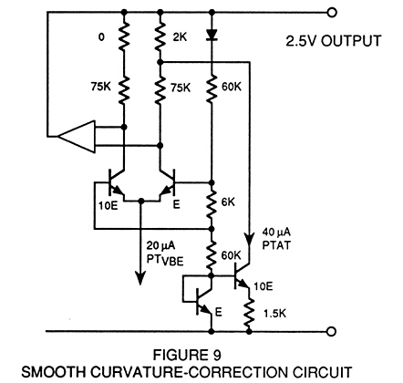
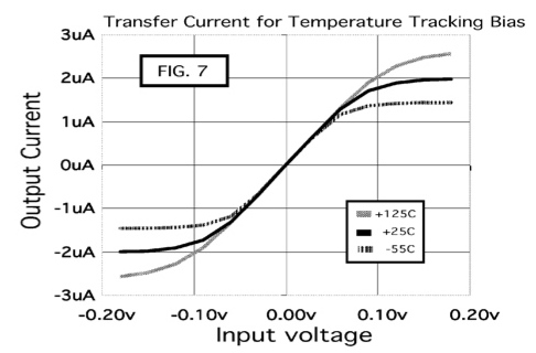
Band-gaps typically take error correction well beyond
first order cancelation. The curvature-correction
circuitry that typically gets added to band-gaps illustrate
that point. Any errors that can be known well enough to
be depended upon are easy targets. But in this case
for the balanced band-gap, it looks like an easy
application" of the old "balancing trick" still had
some life to it.
3.11.10_2.32PM
dsauersanjose@aol.com
Don Sauer
http://www.idea2ic.com/