GROUND FAULT INTERRUPTERS
As of a last shopping trip to a typical hardware store,
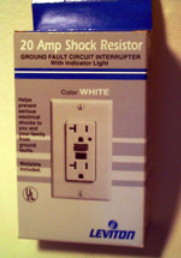
about 50% of the GFIs found to use the LM1851.
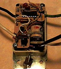
The first version of the LM1851 (LM1850) shown above actually contained
an internal full wave rectifier. The PC board shown below uses a LM1850,
two coils, a few capacitors, a resistor, and the magnetic circuit breaker.
The larger of the two coils shown above was an attempt by Leviton to get
around a patent. It was hoped that a grounded neutral loop could be detected
by running some 60 or 120Hz current through a separate coil. The LM1851
version of this large neutral loop coil is shown below. Provided the neutral
wire is not incorrectly wired to ground, a 5mA imbalance in current between the
two line wires means undesirable current is somehow being shorted to ground.
The problem is at that at such low frequencies, the size and expense of the
large coil is a problem when it comes to inducing 5mA worth of current when the
neutral wire has a 4 Ohm ground loop. A much easier method to sense a neutral
ground loop was to just connect the coils as shown below for the Pass & Seymour
patent.
The polarities of the two coils need to be hooked up such that a 4 Ohm
neutral loop will cause the amplifier to oscillate at about 10KHz. This
required a much smaller and cheaper neutral coil.
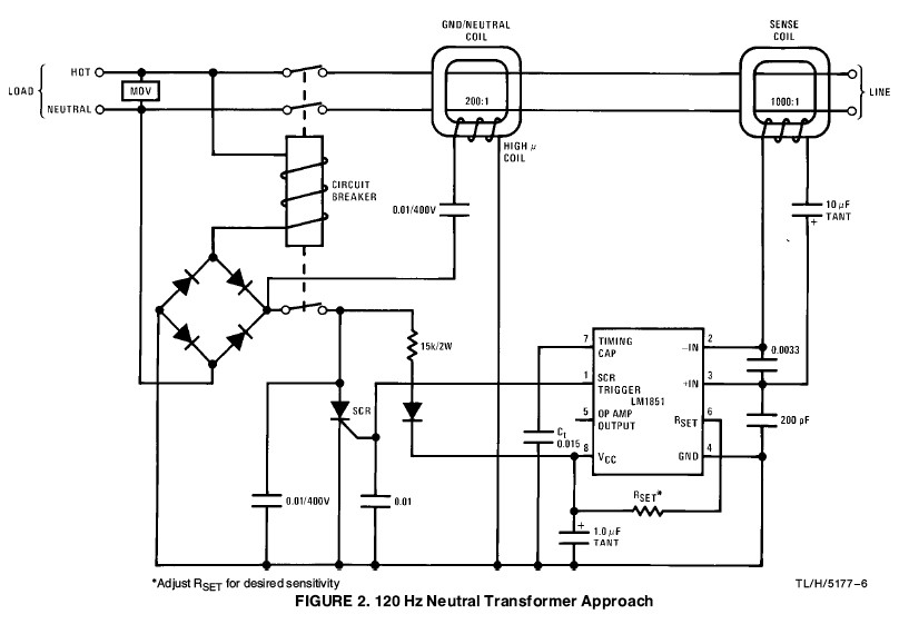
LM1850 SCHEMATIC
The actual schematic for the LM1850 is shown above. The internal
full wave rectifier shown in the upper right of the schematic
was later removed for the LM1851 version because at the time it
was actually cheaper to make the die size smaller and charge the
customer less so he could buy an external full wave rectifier. This
may also improved the GFI's ability to resist false tripping
significantly.
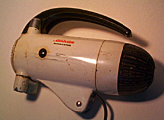
The two intended locations for GFIs was the bathroom and the kitchen.
Right off it was discovered that something like a Sunbeam mixer show
above could fool a GFI into tripping the circuit breaker. To allow the
GFI to avoid false tripping, a timing versus fault current relationship
was specified.
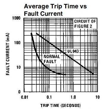
Underwriter's Laboratory had come up with the current versus trip
time relationship that is shown above. At 120Volts, the human
body still has a lot of resistance to current flow even in a bath
tub. Assuming the around 200mA is the worst case, UL wanted the
GFI to trip at about 1/2 a 60 Hz cycle. At the other end, UL listed
5mA as the minimum current and the GFI was expected to trip after
5secs.
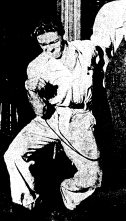
Some of the numbers came from experiments done on graduate students.
For instance the student above is experiencing current well above the
"let go threshold" which is around 10mA. Above 10mA, all muscles in the
body are contracting and the muscle that close a hand are far stronger
than the muscles that can open the hand. Below the "let go threshold"
one can still open one's hand the threshold for sensation is around
1mA. At about 30mAs, the subject's breathing stops.
The GFI timing is decreasing at higher currents mainly because the heart
can go into ventricular fibrillation with only 6uA is applied across it
if applied at a critical time. The fibrillation tests where done with
dogs and scaling was all done based on body weigh. The 5mA limit was set to
simulate an infant. Outside of being able to stop your heart or prevent you
from breathing, 120Volts does little other damage.
The threshold for pain is subjective. From personal experience, 5mA
at 5 seconds is tolerable. I was just a week out of college at the time
when the gentleman below came by me in the lab and showed at lot of interest
in the GFI project. I did not know who this man was at the time and I almost
tried to tempt him to hooked himself up to PG&E for 5 seconds.
The false tripping problem was by far the most challenging. Designing
a GFI to not trip with a SunBeam MixMaster was still not good enough.
Two other GFI ICs before the LM1850 had went into production first.
One of these customers had come up with a way to connect two relays to
oscillate by turning each other off and on such that it became the
acid test. If a GFI design could survive this "Noise Box", then it could
resist false tripping for just about anything.
Unfortunately the "Noise Box" was too good. When it turned on, it made a
terrible racket and messed up all the equipment in the the whole lab.
Can't show a picture of it because one day it mysteriously disappeared.
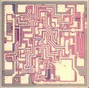
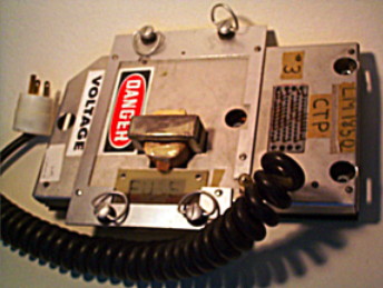
My first independent IC design was a GFI whose die photo is shown below.
The first two GFIs that went into production provided some valuable lessons
for the future of GFIs at National Semiconductor.
The First GFI
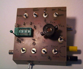
At the time, all linear ICs were tested pretty like Op Amps.
The specifications that were put in the data sheet were all
DC tests. When first silicon came out, a DC lab test box
such as is shown below would be waiting for it.
The Characterization process of first silicon was an attempt to
feel out how an IC would run in production. Things like beta
and resistance would vary month to month. So a spec for a part
needs to have tolerances that allow for these process variations.
Otherwise a month will come along where parts cannot be shipped
to a customer because the wafer sort yields are too low.
At the opposite end, the specs need to be tight enough so that
all parts that ship to a customer are functional. It was soon
discovered that testing GFI ICs like Op Amps could not meet this
requirement. Even with including extra tests and specs which came
from the customer, it was found that maybe one part in 5000
would fail to operate as a GFI. Investigations revealed that this
would usually be due to a devices having two independent defects
which now and again would cancel each other out to allow the
device to pass a DC spec.
Adding more specs and tests would still not be enough. Next the
failure rate might be one in 10,000. Add more tests and then
maybe one in 50,000. The problem was how to predict the highly
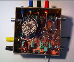
unpredictable. The test system shown below shows how the problem
was solved.
If the device under test however was put into the exact same GFI
circuit and tested to the exact same GFI tests, the customer return
problems went completely away.
As a result of the production experiences which the first two GFIs,
when it came time to ship product to Leviton, they where surprised
National Semiconductor was doing this additional AC testing over and
above the DC tests and specs that were being asked for by Leviton.
But as long as the extra testing did not increase the price of the
part to a customer, they were in effect getting extra testing for free.
It took maybe ten years before Levition realized why the extra
testing was a real economical bargain for National Semiconductor.
When Raytheon started supplying Leviton with GFI ICs, both Leviton
and Raytheon eventually learned just how expensive customer returns
are to both customers and vendors.
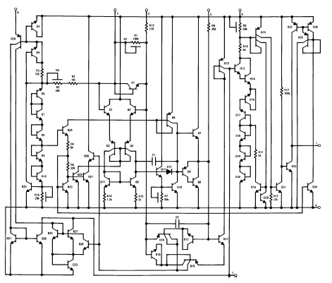
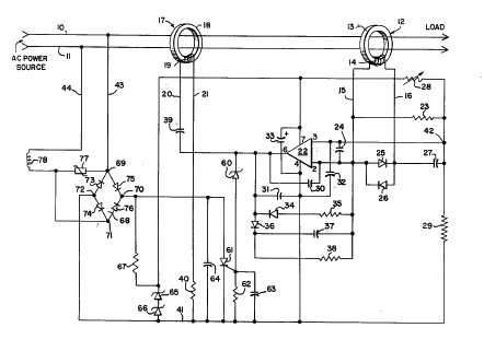
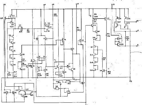
LM1851 SCHEMATIC
The present schematic for the LM1851 is shown above.
The design philosophy was to connect the coil which
is really a 1:1000 turn transformer directly across
the two inputs to an Op Amp. This would make the 1000
turns of the secondary see a virtual ground. As a result,
the ground fault sensing coil would be in current mode
such that a 5mA imbalance in line current would deliver
5uA of current into the summing node of the Op Amp.
The faults signal was now handled as a current to
be processed to match the UL timing spec.
Since the signal was in current mode, it was possible to
do a little extra signal current processing. The circuitry
at the lower left of the LM1851 schematic shows something
called "the three to one pull down". Normally a 5mA fault
would generate 5uA of signal current at the Op Amp's summing
node.
This 5uA AC current would then be full wave rectified
into a capacitor with a DC reference current being pulled
to ground. But since signal was in current mode, it was
possible to sense when the full wave rectified current
exceeded the Op Amp's input bias current, and therefore be
able to triple the DC reference current when no fault current
was present. This may have avoided many headaches.
Back in 1974, GFIs were selling for $70. Today they are not
much more expensive that a normal wall socket. Perhaps at least
a couple of hundred lives in the US are saved each year by their
widespread use. With the introduction of GFIs, the primary
way to get electrocuted switched to workmen on metal ladders.
Now non-conductive ladders are standard.