For a while
it was always a pleasure to see one of my ICs
being sold to hobbyists. Although the LM383 had perhaps a
typical life for an IC, it was sad to see the part being discontinued.
But it is
humorous when the TDA2002 is often referred to
as a replacement for the LM383.
As a matter of fact, the
LM383 is really a reverse engineering of the TDA2002. Credit
should be given to the design engineer Bruno Murari
who was
working for SGS at the time. He was the one who came up with
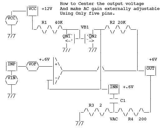
a way to do an automotive power amplifier using only five pins.
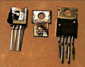
A three lead
version of the TO-220 had been used for voltage
regulators for some time. The new five pin TO-220 had just added
two more pins to the lead frame. But this presented an interesting
problem to the single supply automotive application. Some how the
output pin needed to have a way to center itself between supply and
ground and yet gain of the power amplifier needed to be externally
adjustable. The automotive customers were not allowed to show
anything thing about the TDA2002, but they did give out a clue
as to the part's external circuitry. In particular, the gain feedback
resistors were 220 Ohm and 2.2 Ohm.
Well that hint was enough for Bill
Gross to figure out what SGS must be doing inside. Since this was
a power amplifier, a
high impedance DC negative feedback circuit could center the output
voltage between the rails while a much lower AC negative feedback
circuit could be used to set the audio gain.
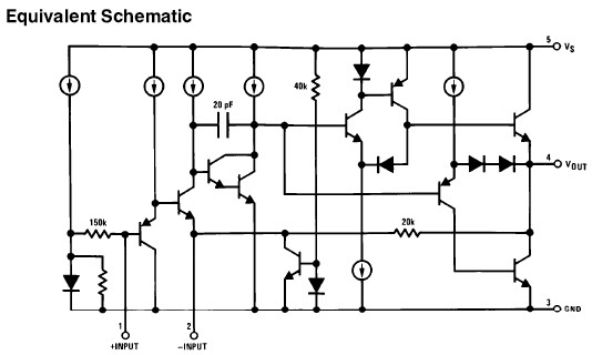
So the LM383
is really a second source of the TDA2002 and it
was completely designed off of a only a hint as to the external
circuitry. Naturally these are two different circuits. But
fortunately they work almost the same. The equivalent
schematic above shows many of the differences. One major difference
was that the LM383 uses only a single NPN to replace the normal
differently input stage. This meant much lower input noise.
Apparently the LM383
works well down at low supply voltage as well.
Now the name of the game was to be
about to put out the maximum
audio power out at automotive supply voltage. But the power
amplifier needs to be connected directly to the car battery.
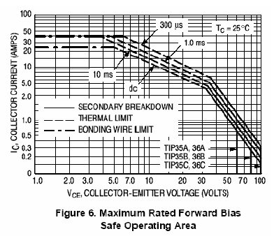
This means that the power amplifier was required to survive
any nasty thing that can be done with a car battery. A Safe
Operating curve as is shown above describes the three ways to
kill a device. Too much current, too much voltage, or too much
power.
The too much voltage issue involve something called "Load Dump".
Cold starting an automotive in subfreezing condition sometimes
involves connecting jumper cables to two batteries connected so as
to double the voltage. The power amplifier was expected to completely
turn off when 24 volts is applied to it's supply pin. This brought
in a patent infringement issue which involved using a series
of zeners to detect the 24 volts. In an attempt to bypass that
patent, the zeners were replaced
by pinch resistors which effectively
did almost the same thing. Apparently this modification worked.
One particular automotive voltage
requirement seems to have taken
care of itself. The auto power amplifier was suppose to be able to
withstand a -6 volts applied across its supply leads. This test was
to allow someone to accidentally connect a car battery up backwards
without doing any serious damage. A person making such a mistake
would know it immediately in that the alternators diodes would become
forward biased and would attempt to short out the battery. The
6volt number represents how well the diodes could shorted out a
car battery. I have seen a physic instructor vaporize a nail with a
car battery.
While the -6 volt supply spec caused little trouble for
the LM383, it meant that all the other electronics in a car needed
to voltage regulator that could provide protection. Some one made
the joke that the lateral PNP's were so bad that even delco would
not be able to destroy them. A skunk works layout of a lateral
PNP regulator ultimately made its way to delco. And sure enough,
they could not destroy it. They loved it. And National Semiconductor
got into the business of making PNP output regulators.
The excess current requirement was handled with current limit circuitry
similar to what is found in the LM741. But in this application
the current requirement was 5 Amps into the smallest area of
silicon as possible. On problem here is the fact that aluminum metal
will actually migrate at high current densities and will ultimately
kill the part. Perhaps this was the first applications at National
Semiconductor to use copper aluminum metal which allowed for a much
higher current density.
The other high current issue involves the bond wires. The fusing current
equation for various wire diameters is given below.
I_fusing = Konstant*dia^(3/2)
For Gold wire in plastic, 1mil wire is can handle 1 to 1.5 Amps and
2mil
can handle 5 Amps. Rumor has it that the gold wire is partially melted
at these currents. Anyway the equation seems to follow the lab results.
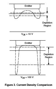
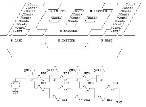
A common issue talked about is the development
of hot spots. In
terms of power transistor layout, to goal was to get all the current
evenly spread out over as large an area of silicon as possible.
A common method to do this was to add degeneration resistors in series
with all the emitters. The layout below reflects that.
At high
currents there is a tendency for current
to be constrained to smaller
and smaller areas.
Being able to resist this effect allows for lower
saturation resistance and makes the output power
transistor less incline to have areas go into
thermal run away. It is common at high currents
for the center of a NPN transistor to turn off
due to current crowding.
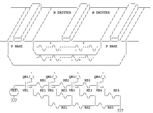
For the
LM383, it was discovered that there already
was a level of IR drop in the right direction and
magnitude which could be slightly modified.
It just so happens that the ratio and
direction of IR
drop in base and emitter is coming close
to tracking
each other at the typical beta level. But this concept
needed to take into account all IR drops.
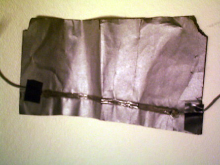
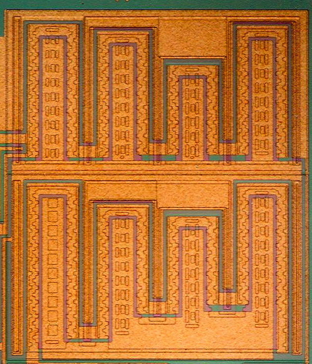
Traditionally the voltage regulator designers had been using
"resistance paper" to layout power transistors like this.
The paper shown below has a resistively in kOhms per
square. Silver conductive paint was used to make
contact to the paper. The paper might be cut or shorted
with conductive paint to reflect the
transistor layout.
Voltages would then be applied. Then someone would use
a DVM to trace out all the voltages on the paper.
Now Days it
is much easier to just use a spreadsheet
to do this as is shown below. The actual
spreadsheet
and its instructions are not
complicated.
But spreadsheets were unknown at this time. So all of the IR drops inside the LM383's
output transistors
were manually calculated and adjusted.
At the 5 Amp level, an output transistor could
be modeled as a parallel of a large number of transistors
each having 250mV worth of degeneration resistance in
its emitter. This makes it a little more difficult
for a single transistor to go into thermal run away.
When a single transistor heats up 1degree, its vbe
drops by about 2mVs. That can cause about an 8% increase in
power, which further increases its temperature.
But with 250mV across its emitter degeneration resistor,
that 2mVs can only increase the emitter current by 1%.
So the thermal run away situation is eight times better.
Now there is also IR drop taking place in all the base
and emitter metal traces. But the emitter region itself
has about 30 Ohms/square resistivity. So holes can be put
in the emitter areas to make local resistance adjustments
to effectively even out the IR drop everywhere. In other
words at the 5 Amp level, all emitter base regions will
be seeing effectively 250mV worth of IR drop from the sum
of IR drops in the base regions or emitter regions or in
metal traces.
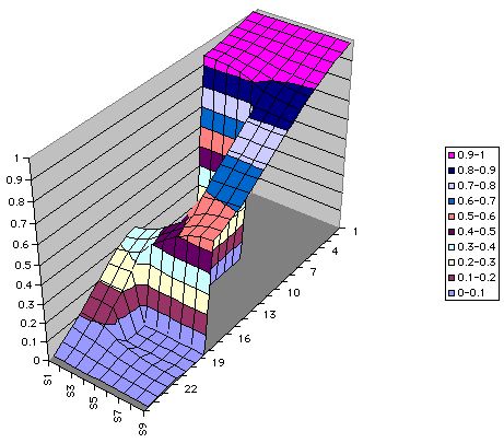
It was
actually possible to measure how well this
current matching worked on a probe station. Liquid
Crystals that change color at various temperatures
could be used to map power dissipation up to maximum
levels provided the power was duty cycled. Apparently
current sharing is good over a 1 to 5 Amp region.
The probe station shown above can run up to full power as
long as it is duty cycled. Otherwise the wire bonds will
"take your picture" in under a second. The resistively of
2 mil gold wire is about 2.4u_Ohms_cm. A 10mil length is
only 0.003 Ohms. But its mass is so small that 5Amps can
heat up to its boiling point in under 60msec.
The last
remaining safety issue is the thermal shut down
circuit. It is common to design the whole circuit to
start shutting itself down around 125C. It once was thought
that the two worst tests where to short the output pin in
all conditions with either the very good heat sink or a
very poor heat sink. With a good heat
sink, the part won't
get up hot enough to turn on thermal shutdown. But the current
limit will allow a part to survive 1000 hours. With a poor
heat sink the thermal shut down will kick in and protect the
part for 1000 hours. Then
Chrysler came along and showed that
it was possible to have an in between heat sink that really
is the worst case.
For reasons
of curiosity, the protection circuitry was
disabled on some parts that were built using the first
TO-220 package. A destroyed part is shown in two pieces above.
There appears to be a consistent power density where plastic
will neatly pop off of silicon. From the previous Chrylser
simulation, applying 45 watts to a 22x42mil output NPN
transistor
appears to put it at least to 160 degrees C in a very short time.
The plastic is probably designed to expand over temperature
with everything else. But the plastic will pop off in a fraction
of a second, and plastic is not a good conductor of heat. Either 45Watts
to one or 90watts to both appears to pop the plastic off the silicon
with out any apparent damage to the chip. Now it is no longer possible
to do this since the packaging department had redesigned
the package to look like what is shown above to the right. Today metal
pieces from the heat sink hold on to the plastic to keep the
part in one piece when it blows up.
The ability to blow up is a bit unnerving in that you never know
when it is going to happen. This part at first was hand tested
on the test floor. Even though the part now would remained in
one piece, the women on the test floor insisted that a little
box should be hinged to the test fixture such that it would always
go over the part during test.
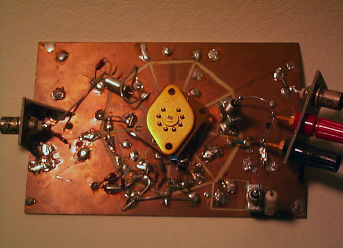
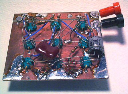
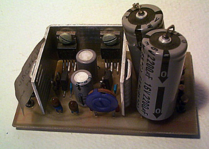
Above is a
simple example of a bread board. During this
time, the lab actually had carpets which enable a
person to deliver a pretty good shock. A power amplifier
bread board was one of the few bipolar bread boards
which actually could go up in smoke with a good zap.
The power requirements for the bread board meant that
the current limits and voltage levels needed to both
be set high. A particular Product Engineer Manager was
fond of clapping his hands behind anyone working
with power.
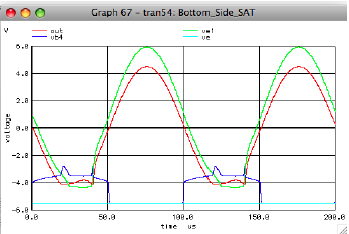
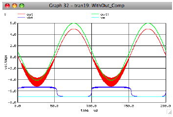
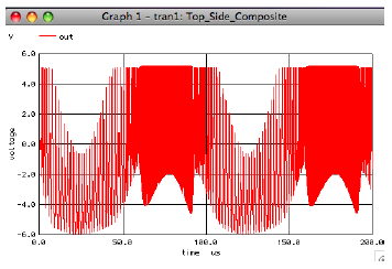
But "Bottom
side Fuzzy" is usually the most obvious complaint.
The old lateral PNPs are barely functional. Since
it was not possible to pull 5 Amps to ground using a PNP,
it had to be done using a PNP composite, which could be
counted on to oscillate. But this often could be corrected
by connecting a R and C comp circuit between the output
and ground.
The assumption being made is that R and C comp
circuit
uses the "short lead rule".
Failing to observe this
rule has resulted in some customers attempting to
stabilize the output stage with an inductor.
Now in the case of an Automotive Audio application,
it really would be optimum for the output to be
a rail to rail output. Since PNPs can not put out
much current, the top side will have to be a NPN.
But to get the most out of that NPN, it will have to
have its base be driven by a PNP. And that is a top side PNP composite which
is even less stable than
the bottom side composite.
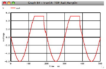
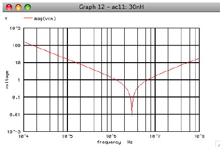
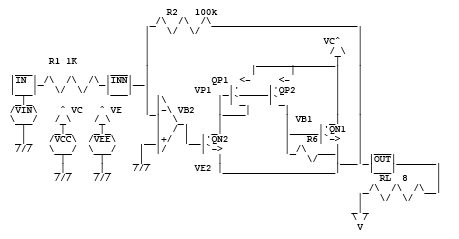
This top side stability problem was
solved as is
shown in the equivalent schematic below. The
application still required a NPN that could put
out 5Amps. And a big PNP was still needed to
drive it. It's just that those two transistor
don't have to be put into a loop.
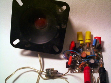
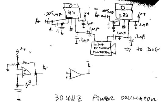
Now if one
really wants some audio power in
your car, one can hook up a bridge.
My office
mate decided to make four bridges for the four
speakers in his BMW. For some reason he wanted
us to listen to them at full power with the
windows rolled up. Having your ears ring
afterwards is probably not a good thing.
I had found
an alternative application for the
bridge. My neighbor had just got a dog that was
always barking. So I got tweeter, built
up a simple 30kHz oscillator using a LM324.
Set the two LM383 to swing rail to rail.
Got a lantern battery that could put out
the power. Then connected the tweeter.
It may not
be a good idea connecting the tweeter
when it is facing you. You can't hear anything.
But your ears will ring. Once turned on,
you will not only hear all the dogs in your
neighborhood bark, the next block over will
be barking too.
So the
frequency of the oscillator gets adjusted to
maximum barking frequency. The tweeter then gets mounted
high and between the houses. An ON/OFF power switch was
rigged up so my wife could carry on a silent conversation
with the dog. In this case the circuit appeared to be
effective at discouraging the barking without the
neighbor knowing. Don't know the long term effects
because the neighbor shortly got rid of the dog.