A Fast and Simple Asynchronous ADC
(Auto-Folding Multi-Bit Comparator)
(US Pat. 7839317)
This invention could have been invented in the late 60's.
Would a high speed comparator which provides a multi-bit output been
useful back then? And the architecture is simple and all NPN.
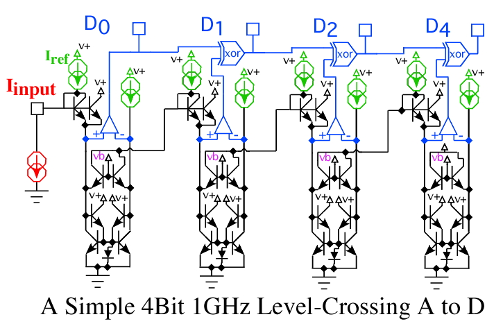
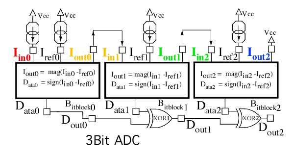
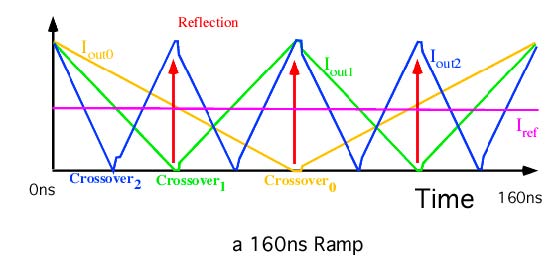
The circuit shown above is actually the full schematic for a 4 bit 1GHz
asynchronous level crossing A to D. The digital elements shown in
blue are not drawn at transistor level since differential logic
needs to be used. All the DC reference currents shown in green
match each other in current value. All NPNs are minimum 1X geometries,
and the reference currents are chosen to run all NPNs at their
maximum ftau. The analog input shown in red is an input current having
a full scale range from zero to the reference current level.
When the NPNs are modeled as having a ftau at 4GHz, the digital output
response to a full scale 16ns ramp input current is shown below.
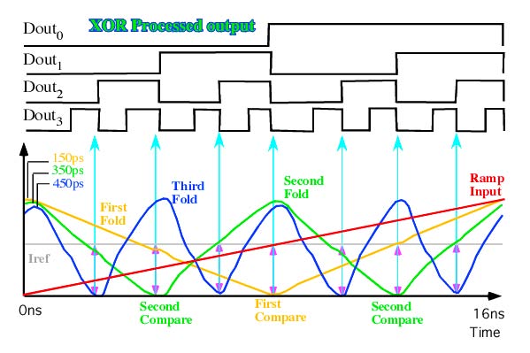
Each cell is doing a current comparison to the reference current,
but it is also outputting a folded version of the analog signal current
as well. Some simple first order speed up techniques have been applied
to allow 4GHz NPNs to track a moving input with no missing
codes at a 1GHz rate. Some much better modeling, and some more advanced
speed up techniques might allow the LSB tracking output code rate to come
even closer to the ftau of the transistors.
The XOR logic circuit is reformatting the digital output into
the normal binary format. Notice how when the MSB reverses state,
all the other bits need to reverse state at the same time.
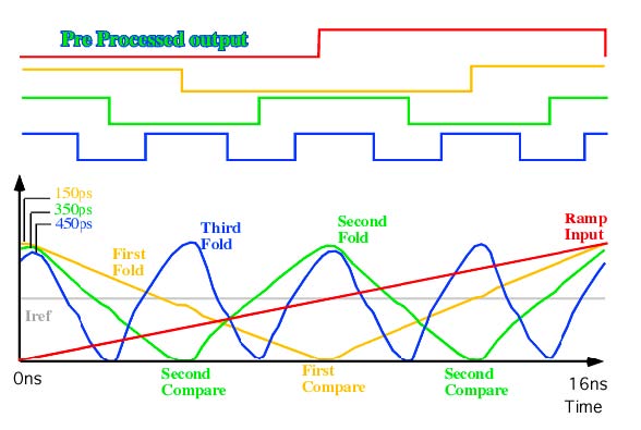
The pre-processed digital output has an interesting format.
Only one cell is able to switch state at a given time.
When any of the cells switch state, all the other
cells are stationary. So a single output state change
could trigger all the bits to be cleanly sampled. The
XOR function can then be applied later at any time.
The comparator cell was actually invented as a way to perform
an absolute value function on two input current sources (4,069,460).
It has since then found other uses, such as for a precise AM decoder
for use in an AM stereo decoder (4,359,693).
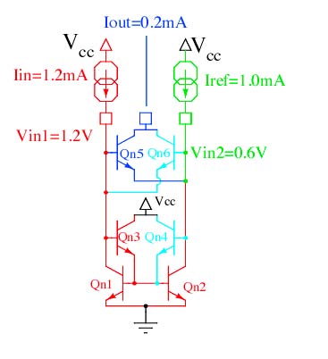
The circuit is essentially a dual input current mirror in which the larger
of two input currents take over the current mirror. Some voltage clamping
transistors prevent saturation while provide an output current
equal to the absolute difference between the two input currents.
If Iin is 0.2mA larger than Iref, 1.2mA will flow in Qn1 and Qn2.
Transistors Qn4 and Qn6 will be off. And transistor Qn5 will make up
the 0.2mA difference in input current.
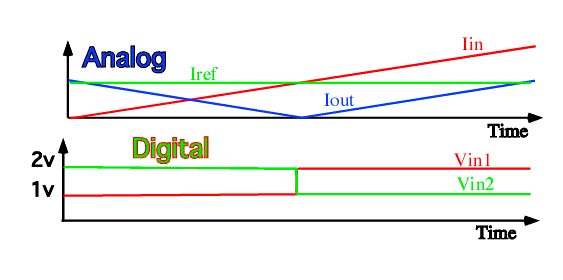
Now if the Iin current is ramping up, it becomes obvious that
the input current is both being compared and folded at the
output at the same time. The comparator's differential input voltage
will toggle around the reference current, and can be used as a
differential digital output port. The absolute value output current
happens to be the input current folded around the reference current.
This folded output current can be sent to another stage, and
the analog signal gets compared and folded a again.
The current processing of the signal is mathematical. Each stage
compares the current between an analog input current and a
reference current. The analog input current further gets
folded to an absolute value of the difference between the two
input currents. This folded output current can then be passed
on to a series of following stages.

But the folding of the analog signal is being done just like
it would be done on a piece of paper. Every fold means a
half reduction in magnitude. This means that the reference currents
will have to be reduced by a factor of two at each stage. A need
for speed makes it desirable to use minimum geometries for all
transistors in the signal path. And all the transistors need to operate
at an optimum current level to have a maximum ftau.
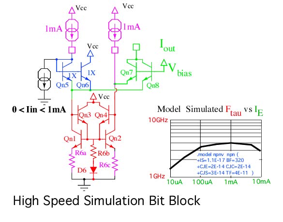
Some simple first order techniques to address speed issues are
shown in the circuit above. Transistors Qn6 and Qn5 make up for
the gain reduction happening at each current fold. A NPN transistor
which has a 4GHz ftau is being used as a model. This NPN has an
optimum ftau around 1mA. Transistors Qn1 to Qn4 all want to
be biased up to run as fast as possible. Diode D6 and resistor R6b
are biasing Qn3 and Qn4. Degeneration resistors at Qn1 and Qn2 may be
desirable to enhance matching.
The biggest problem is when a transistor turns off, it often
takes a while to turn back on. So transistors Qn7 and Qn8 have
pick up the additional job of being clamping diodes. The voltages
between the bases of Qn3 and Qn4 is the actual digital output.
These nodes are going to want to go to some differential logic
stage. Raising the Vbias voltage applied to Qn7 and Qn8
will begin to limit the voltage swing of the differential digital
output. So Vbias can control the degree to which transistors
like Qn3, Qn4, Qn7 and Qn8 can turn off. So how little of a input
voltage does internal differential logic need? A swing around
+/- 50mV between the bases of Qn3 and Qn4 might be a good place
to start.
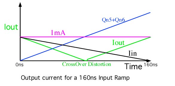
Whenever something turns off, it will have a little delay
at turning back on. In amplifier applications, this is often
called cross over distortion. It will create a glitch for
a short amount of time. Biasing transistors to stay on will
reduce this effect.

Using the higher speed cells, the connection of the cells
has becomes easier. Everything gets biased to the same reference
current of 1mA. This tends to biases all NPNs at a maximum ftau.
The crossover glitches have a convenient format. They appear
to want to distort all the folded analog waveforms at their
endpoints. This is convenient in that the critical current
comparison is always happening at the center of the folded
waveforms.
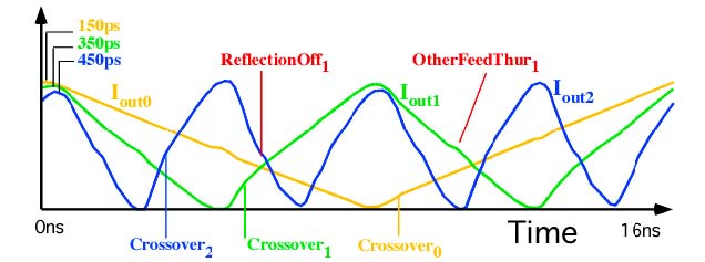
But folding every stage means that currents get toggled
twice as fast for every bit stage. When toggling speeds approach the
ftau of the transistors, the crossover glitches may no longer
be at just the endpoints. At high enough speeds, they begin
to migrate away from the endpoints, and start interfering with
the current comparison process.
This is an interesting type of failure. It means that missing
lsb codes starts to appear at higher input slew rates. So there
is a bit resolution versus input slew rate tradeoff. Put in a
faster moving analog signal, and get a lower bit resolution
digital output.
Simulation suggests that 4 cells can track a 16nsec full
scale ramp and produce all 16 individual LSB codes at a rate
of 1GHz per LSB. The ftau for the NPNs is only 4GHz. Only
some simple speed up techniques were used to do this. Just
how close the conversion rate can come to matching ftau
is going to require an exception ability to match silicon
to spice models.
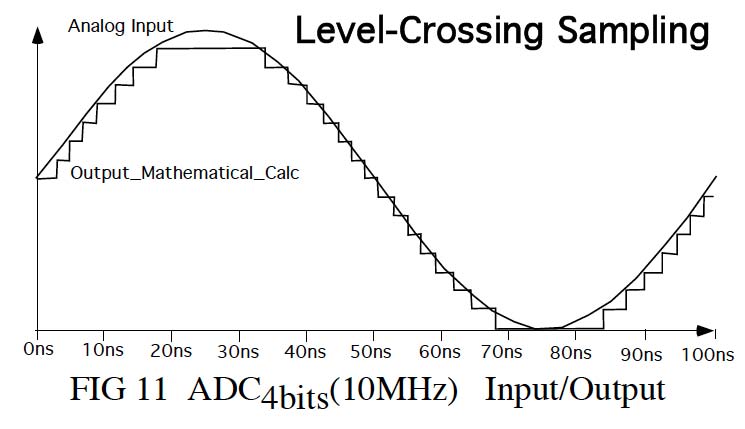
Apply a Full scale 10Mhz sine wave to the input, and then mathematically
reconstruct the digital output back into a analog waveform. This shows
that the output transitions are not happening at a periodic rate. In some
applications, this has the benefit in that the digital output is only
changing state when something is actually happening.
This kind of digitizing of analog signal has been referred to as
level crossing sampling, or as a threshold crossing detector,
or as an Asynchronous Analog-to-Digital Converters,
or even as a Level-Crossing Flash Asynchronous Analog-to-Digital Converter.
Where as a normal A to D stores it resolution in terms of a precise voltage
level, this type of converter stores its resolution in terms of
a precise time when something has happened. There has been some interest
in using this type of a converter lately. The following are some recent
examples of Asynchronous ADC activity off the web.
6
bit Asynchronous December 2006
Asynchronous
ADC In CAD Mentor Graphics
Asynchronous
Data Processing System
ASYNCHRONOUS
PARALLEL RESISTORLESS ADC
LEVEL BASED SAMPLING FOR ENERGY CONSERVATION IN LARGE NETWORKS
A Level-Crossing Flash Asynchronous Analog-to-Digital Converter
Weight functions for signal reconstruction based on level crossings
Adaptive Rate Filtering Technique Based on the Level Crossing Sampling
Adaptive Level–Crossing Sampling Based DSP Systems
A 0.8 V Asynchronous ADC for Energy Constrained Sensing Applications
Spline-based signal reconstruction algorithm from multiple level crossing samples
A
New Class of Asynchronous Analog-to-Digital Converters
Effects
of time quantization and noise in level crossing
sampling stabilization
Here is some more background information on Analog to
Digital converters.
A
1-GS/s 6-bit 6.7-mW ADC
A
Study of Folding and Interpolating ADC
Folding_ADCs_Tutorials5
high
speed ADC design
Investigation
of a Parallel Resistorless ADC
Here are some patents on the subject.
4,291,299_Analog_to_digital_converter_using_timed
4,352,999_Zero_crossing_comparators_with_threshold
4,544,914_Asynchronously_controllable_successive_approximation
4,558,348_Digital_video_signal_processing_system_using
5,001,364_Threshold_crossing_detector
5,315,284_Asynchronous_digital_threshold_detector_
5,945,934_Tracking_analog_to_digital_converter
6,020,840_Method_and_apparatus_for_representing_waveform
6,492,929_Analogue_to_digital_converter_and_method
6,501,412_Analog_to_digital_converter_including_a_quantizers
6,667,707_Analog_to_digital_converter_with_asynchronous_ability
6,720,901_Interpolation_circuit_having_a_conversio2
6,850,180_SelfTimed_ADC
6,965,338_Cascade_A_D_converter
7,133,791_Two_mean_level_crossing_time_interval
This is a different type of style of ADC. (Event
Sampling)
About
Folding ADCs
An
easy architecture to perform the same function
Folding
and Flash
architectures have been around for some time
But none
this simple.
Level
Crossing + Asynchronous
ADC follows different rules
AADC
sampled with a clock, is normal ADC
Threshold
Sampling may look like it is truncating data.
An
easy extrapolation method is shown here
More advanced
methods are found here.
Extrapolation
actually works quite well.
Additional
Event Sampling to Threshold Sampling.
11.19.10_1.20PM
dsauersanjose@aol.com
Don Sauer