*=============Sweep_Load_ChargePump=======================
Sometimes being able to sweep a simulation condition over several
orders of magnitude is needed to see when something gets into
trouble. For instance, this method is apply to an Op Amp's output
loading to verify operation. Viewing the output versus time can
show that a sweep can catch conditions when things are marginal.
Using a piece wise linear voltage source, a voltage can
be ramped up several orders of magnitude. This voltage can then
be converted to a current source that is applied to an output node.
While the ramp up is not linear on the log scale with respect to time,
the full dynamic range of the sweep is covered to verify that something
works over an entire range.
=======================================================================
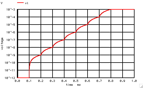
VL VL 0 PWL ( 0 1p .1m 1p .2m 1n .3m 10n .4m 100n .5m 1u .6m 10u .7m 100u .8m 1m )
BLOAD OUT 0 I = v(VL)
=======================================================================
Plotting this voltage over time shows that "VL" it is not a
perfectly linear log ramp up. But it comes close enough.
The values for VL and BLOAD are chosen so that the load
current applied at the output "OUT" is scaled to amps.
=======================================================================
Charge_Pump
* ___ D1 VD1 D2 VD2 D3 VD3 D4 ___ ROUT
* |VCC|__|\|_________|\|_________|\|_________|\|___|OUT|__/\ /\ /\__
* |___| |/| _|_ |/| _|_ |/| _|_ |/| |___| \/ \/ _|_
* C1 ___ C2 ___ C3 ___ C4 _|_ ///
* ___ |\ | |\ | |\ | ___COUT
* |CLK|_| \/\___|___| \/\___|___| \/\___| |
* |___| | /\/ V1 | /\/ V2 | /\/ V3 _|_ 5pF caps
* |/INV1 |/ INV2 |/ INV3 ///
*
=======================================================================
A CMOS charge pump such is shown above might find application
in developing internal 15volt supplies inside ICs that are
running off of 5 volt supplies. Programing internal EEPROMS
often need such internal voltages.
So if 5pf internal capacitors are being used, and the switching
is being done at 1MHz, how much of a current load can this charge pump
handle?
The switch capacitor equivalent resistance equation is as follows.
R_eq = 1/(freq_clock*C)
= 1/(5e-12*1e+6) = 200KOhms
=======================================================================
Charge_Pump
* ___ D1 VD1 D2 VD2 D3 VD3 D4 ___ ___
* |VCC|__|\|_________|\|_________|\|_________|\|___|OUT|___| _|_
* |___| |/| _|_ |/| _|_ |/| _|_ |/| |___| / _ \
* C1 ___ C2 ___ C3 ___ C4 _|_ \/ \/
* ___ |\ | |\ | |\ | ___COUT /\_/\ BOUT
* |CLK|_| \/\___|___| \/\___|___| \/\___| 5pF caps | \___/
* |___| | /\/ V1 | /\/ V2 | /\/ V3 _|_ _|_
* |/INV1 |/ INV2 |/ INV3 /// ///
*
VL VL 0 PWL ( 0 1p .1m 1p .2m 1n .3m 10n .4m 100n .5m 1u .6m 10u .7m 100u .8m 1m )
BLOAD OUT 0 I = v(VL)
So this is where a large dynamic range sweep might come in handy.
First wait for the charge pump to settle. Then ramp up a load current
=======================================================================
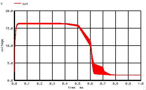
One can see that the output voltage is really
dropping at .6msec.
At that time, the load current is at 10uA.
A 10uA load current corresponds to a 5.7volt
drop in output voltage. That corresponds to
about an output impedance of 570kOhms. Which
is about three times larger than the equivalent
resistance of a single 5pf capacitor switching at 1MHz.
===========Full_Netlist_For_Copy_Paste=======================
Charge_Pump
* ___ D1 VD1 D2 VD2 D3 VD3 D4 ___ ROUT
* |VCC|__|\|_________|\|_________|\|_________|\|___|OUT|__/\ /\ /\__
* |___| |/| _|_ |/| _|_ |/| _|_ |/| |___| \/ \/ _|_
* C1 ___ C2 ___ C3 ___ C4 _|_ ///
* ___ |\ | |\ | |\ | ___COUT
* |CLK|_| \/\___|___| \/\___|___| \/\___| |
* |___| | /\/ V1 | /\/ V2 | /\/ V3 _|_
* |/INV1 |/ INV2 |/ INV3 ///
*
.OPTIONS GMIN=1p METHOD=gear ABSTOL=1u TEMP=27 srcsteps = 1 gminsteps = 1
.OPTIONS RELTOL=.001 ABSTOL=1n VNTOL=1n ITL4=500 ITL1=400
*======== ====== ====== ====== ====== ====== ====== ====== ======
VCC VCC 0 DC 5
VCLK CLK 0 DC 0 PULSE( 0 5 1p 1n 1n .5u 1u )
VL VL 0 PWL ( 0 1p .1m 1p .2m 1n .3m 10n .4m 100n .5m 1u .6m 10u .7m 100u .8m 1m )
BLOAD OUT 0 I = v(VL)
XINVR1 CLK V1 VCC INV
XINVR2 V1 V2 VCC INV
XINVR3 V2 V3 VCC INV
D1 VCC VD1 DD
D2 VD1 VD2 DD
D3 VD2 VD3 DD
D4 VD3 out DD
C1 VD1 V1 5p
C2 VD2 V2 5p
C3 VD3 V3 5p
C4 OUT 0 5p
ROUT OUT 0 10meg
.control
set pensize = 2
tran 1u 1m 0 1u
plot out
plot vl ylog
plot vd1
plot vd2
plot vd3
.endc
*=========The_CMOS_Model_Files==================================
.model NMOSC NMOS(Level= 1 Cbs=2f Cbd=2f)
.model PMOSC PMOS(Level= 1 Cbs=2f Cbd=2f)
.model DD D(IS=3.15e-18 )
*=========Inverter============================================
* ^
* INV_R /_\ VCC
* |
* <-
* ||___
* __|| XINVR A OUT VCC INV
* ___ | ||_ MP1
* |VIN|__| | ___ ^ VCC
* |___| | |__|OUT| /_\
* | _| |___| |\_|
* |__|| ___ | \ __ ___
* ||___ MN1 |A |_| \/ \_|OUT|
* ||-> |___| | /\__/ |___|
* _|_ | /
* /// |/
*
.SUBCKT INV A OUT VCC
MN1 OUT A 0 0 NMOSC W=1u L=1u
MP1 OUT A VCC VCC PMOSC W=3u L=1u
.ENDS INV
.end