This invention concerns itself with what happens when
a
large number of transconductance amplifiers get put into
the same integrated circuit. Having a pre-distortion or linearizing
circuit at the input to a transconductance amplifier is
actually performing a critical function in addition to
lowering distortion. They are also performing a temperature
scaling function.
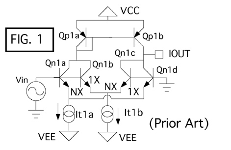
The linearizing diodes used in the LM13700 were suited
to a +/-15V supply world. Signal levels were often set
to several volts. At such levels, resistors could be
used without introducing much noise, or distortion, or offset.
What may not be obvious is that the linearizing diodes
are also gain scaling the input signal of a transconductance
amplifier to track absolute temperature. This is important
because the current to voltage relationship of transconductance
amplifiers happen to decrease relative to absolute temperature.
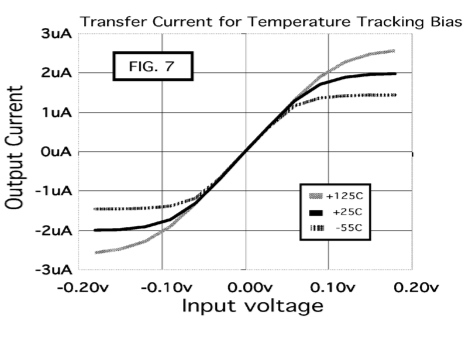
A simple plot of the transfer function of a two transistor
input stage can show that relationship.
Temperature gain balancing is happening when any type
of linearizing or pre-distortion circuitry is applied to
the input of a transconductance amplifier. But what happens
when a transconductance amplifier input stage is using
distortion cancellation, and does not use a pre-distortion
circuit?
The transfer circuit for the circuit above still has its
gain dropping relative to absolute temperature. But the
distortion curves shown below shows that the distortion versus
input signal is also highly temperature dependent.
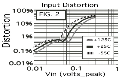
Normally the input level gets picked as a trade off between
distortion and signal to noise. Without any pre-distortion
circuitry, there is now a temperature relationship associated with
distortion.
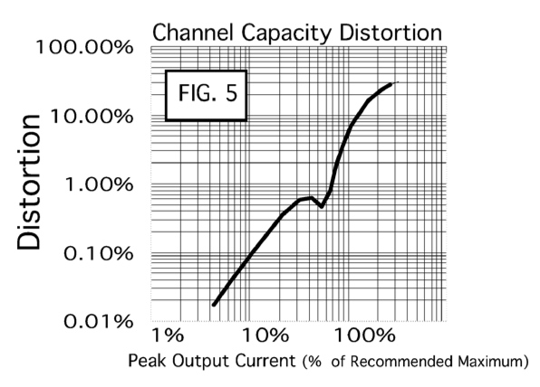
If signal is instead treated in terms of being a percentage of
the maximum output current, then both temperature
and bias current are removed from the transconductance
amplifier's distortion curve. Think of the maximum output
current as being its channel capacity.
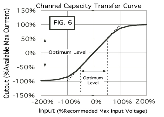
A 50% rule can be used to relate an output current
capacity to an effective input voltage capacity.
Transconductance amplifiers are usually pretty
linear up to the point where their putting out
around than 50% of their maximum output current.
Define the input voltage to be at its 50% maximum
input level when its output current is at 50% of
its maximum output level. So maximum input capacity
voltage for that input stage can be treated as twice
that 50% level.
Using transconductance amplifiers to build things like
voltage controlled filters can show that thinking of
signal in terms of either voltage levels or current levels
is going to get confusion, especially when trying to maintain
an optimum distortion levels versus signal to noise ratios over a
-55C to 125C temperature range. Thinking in terms of
percentages of channel capacity can make things much easier.
Think of a transconductance amplifier operating at 50%
capacity as putting out current at 50% of its maximum
output current, and having an input voltage being
applied which is at 50% of the recommended input level.
Now regardless of the bias current for the transconductance
amplifier, it will still be operating at 50% capacity. If the
input voltage gain is set to track absolute temperature,
then operating at 50% channel capacity will be independent
of both the transconductance amplifier's bias current
and temperature.
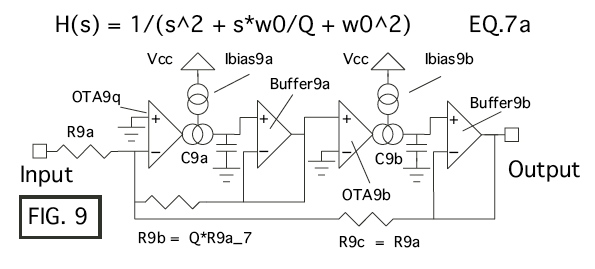
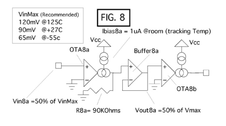
In in the schematic above, assume all resistors have zero
temperature coefficients. How the bias current for the
transconductance amplifiers get generated is key.
Suppose the 1uA current is derive from a collector current of
an NPN transistor which has its base connected to a bandgap
and has a 600K resistor from its emitter to ground. This will
force a temperature tracking 600mV across a 600K resistor. By using
a 90KOhm resistor at the output of the first transconductance
amplifier, it automatically supplies an output signal
to the second transconductance amplifier with a signal
in the same 50% channel capacity format. And this can be apply
onward to a further series of transconductance stages.
Things however may look a little strange when looking at
the transfer curves of the transconductance amplifiers.
Over temperature, they will all have the same slope.
In other words, the current to voltage relationship
resembles a resistor which has a zero temperature coefficient.
But output current capacity and for that matter the
input voltage capacity will all increase as absolute
temperature increases. So if the input signal also
tracks the channel capacity, then the signal will operate
at a fixed percentage of channel capacity regardless of
temperature. In this special case, the current to voltage
relationship (impedance) is temperature independent. The
signal levels in terms of percentages of either currents or
voltages are also temperature independent.
Now assume all resistors will increase exactly 33.3% for
a 100C increase in temperature. Now when the 600mV is applied
across the 600K resistor, the 1uA current will remain constant
over temperature. But the current to voltage relationship
for the transconductance amplifier will look like a resistor
which is increasing by 33.3% for a 100C increase. So this will
introduce a 33.3% reduction in output current. But in this
case, the 90K resistor will also be increasing 33.3%. So
the output voltage gain will still be able to drive the following
transconductance amplifier at 50% capacity. So both
transconductance amplifiers will still be operating at 50%.
Two details should be noted. The TC of the resistor used to
generate the bias current for a transconductance amplifier
will define the TC of the transconductance amplifier. If the
TC of the transconductance amplifier matches the TC of the
load impedance at its output, then signal in terms of a
percentage of channel capacity can be maintained from stage
to stage.
So the TC of the resistor which has 600mV forced across it
only needs to match the TC of the load impedance. This
is also possible for voltage controlled filters. The TC of
capacitors is near zero. Using a Sichrome resistor would
come close to matching the zero TC.
Transconductance amplifiers appear to want to work in a
dimension less or pure ratio mode. For instance the bias current
applied to a transconductance amplifiers, makes is act like a
resistor, which is set to a ratio of the impedance loading its output,
and defines a temperature independent input to output gain. Changing
the bias current is only changing the ratio. For filters,
the load impedance is a capacitor. This means gain versus
frequency is temperature independent.
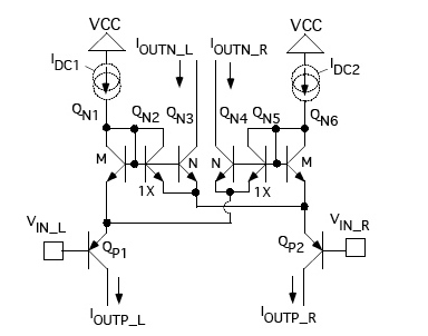
________________________________________
| VCC | | VCC | _|_
| | | | /VCC\
-> <- -> <- \___/
QP1`|___|'QP2 QP4`|___|'QP5 _|_
_ '| | |`_ _ '| | |`_ ///
| |____|VTA2 | |____|VTA5
| | | |
| <- | <-
|_______|' QP3 _____|_______|' QP6
|VTA1 |`_ | VTA4 |`_
| | | | OUT
| 510nA |_____/|\___ | 490nA 20nA
| | | | R1 1 Ohm
| 490nA ______| | |___/\ /\ /\_
Vin = +1mV _| |_ | VTA6 _| \/ \/ |
__|'QN1 QN2 `|__ |________|'QN5 _|_
_|_ |`-> <-'| _|_ | |`-> 510nA ///
/VIN\ | | /// | |
\___/ |__________|VE | ______| VTA7
| _|_ _____ |_ | _|
_|_ / _ \ _|_ _|_ QN3`|__|__|'QN4 20nA/1uA = 2%
/// \/ \/ /VEE\ /// <-'| |`->
/\_/\ \___/ | | 1mV/51mV = 2%
\___/ _|_ _|_ _|_
IBIAS _|_ \ / \ / \ /
1uA \ / V VEE V VEE V
V
The DC offset remains at a fixed ratio of the channel capacitance.
For instance, a 1mV input offset represents a 4% mismatch for a
two transistor input stage. This will in fact produce a 2% DC offset
at the output current port which is independent of bias current or
temperature. Using the 50% rule, this type of input has a capacity
of 51mV. So the DC offset is a 2% error relative to both the voltage
input or current output. A 1mV input offset will increase with absolute
temperature. This is where input offset temperature drift comes from.
So if signal is handled as a percentage of both the voltage input
or current output channel capacity, then in theory there is no DC
temperature drift.
ShotNoise_I_rms = sqrt(2*q*I_dc*BW)
Signal/Noise = I_dc/sqrt(2*q*I_dc*BW)
= 1/sqrt(2*q*BW/I_dc)
= 1/sqrt(2*q*BW/q*Num_electrons_per_sec)
= 1/sqrt(2*BW/Num_electrons_per_sec)
The noise in a transistor differential stage is mainly all shot noise.
The signal to noise ratio is really defined by the bias current or number
of electrons per second that bias up the transconductance amplifier.
Signal to noise ratio can really only be related relative to the
maximum output current. And the signal to noise ratio will double
for a 4X increase in number of electrons per second.
There are different types of input stages. The stage above has an input
voltage capacity of 196mV. All transconductance input stages have a
distortion profile that can be made independent of temperature, provided
the input signal is applied in terms of being a percentage of the available
capacity. So everything can be temperature independent in the percentage
format. That includes signal, dc offset, gain, frequency response,
distortion, and "almost" signal to noise ratio. Unfortunately resistors
inside ICs increase closer to 20% rather than 33.3% over 100 degrees C.
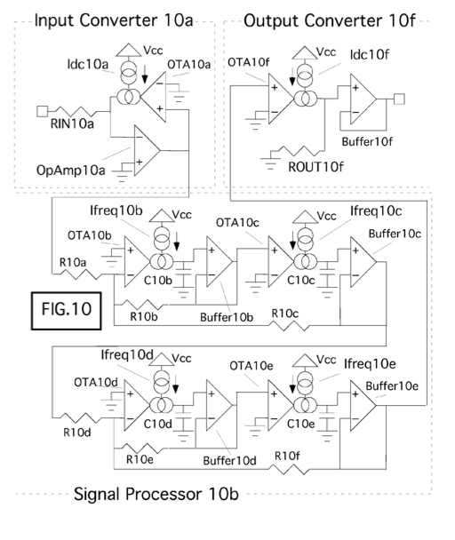
This invention concerns itself with what happens when a
large number of transconductance amplifiers get put into
one integrated circuit. One could solve both
distortion and temperature scaling issues by putting
pre-distortion circuitry in front of every transconductance
amplifier. Or one could handle signal in terms of percentages
of channel capacity, and use distortion cancellation inputs.
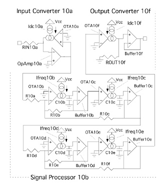
The schematic shown above has the Input Converter using
a feedback loop to pre-distort and scale the voltage. Using
negative feedback has its advantages. There are ways to do the
job open loop. One pre-distortion stage may always be needed to
convert voltage magnitude to a percentage of channel capacity.
But after the signal is in percentage format, no more pre-distortion
stages are needed. The conversion from percentage format back to
voltage magnitude can easily be done by simply biasing up the last
transconductance amplifier with a more temperature independent
current.
3.11.10_2.37PM
dsauersanjose@aol.com
Don Sauer
http://www.idea2ic.com/